Silicon wafer manufacturing process
At the heart of today’s groundbreaking technological advancements lies the unsung hero - the silicon wafer. This crucial component, born from the meticulous process of silicon wafer manufacturing, stands as the foundation upon which the electronics industry builds its innovations. Silicon, transformed into a pure, flawless crystal through sophisticated production techniques, is the key semiconductor material that powers our digital world. The production of these wafers is a marvel of modern engineering, enabling the creation of smaller, faster, and more efficient electronic devices. As the backbone of semiconductor technology, silicon wafers are not just pieces of crystal. They are the canvas on which the future of technology is painted. Embrace the power of silicon wafer technology and step into a world where the possibilities are limitless, driven by the precision and innovation of silicon wafer manufacturing.
A brief description of the history of silicon wafer production
In the mid-20th century, scientists discovered that silicon, a common element found in sand, had the potential to revolutionize electronics. They began experimenting with ways to purify silicon and turn it into a crystal form, which laid the groundwork for the first silicon wafers.
As decades passed, the process of making silicon wafers became more refined. Techniques such as the Czochralski process allowed for the growth of large, single-crystal silicon ingots, which could then be sliced into thin wafers. This was a game-changer, enabling the mass production of silicon chips and paving the way for the rapid advancement of computers, phones, and countless other gadgets.
Throughout the years, the quest for smaller and more efficient chips led to innovations in both deposition and etching techniques, making circuits tinier and more complex. These advancements were not just technical feats. They were milestones that mirrored the fast-paced evolution of society's needs and technological dreams.
The history of silicon wafer production is a rich tapestry of scientific curiosity, technological challenges overcome, and visionary thinking. It’s a testament to how far we've come from the early days of computing, powered by the continuous improvement and ingenuity in silicon wafer manufacturing.
Overview of silicon wafer applications
Raw materials
The fascinating history of silicon wafers begins with the humble raw materials that lay the groundwork for this revolutionary technology. The journey to a finished chip starts with the purification of silicon, a process that transforms raw silicon into highly pure polycrystalline silicon, the cornerstone of semiconductor production. This high-purity material then undergoes the magical process of crystal growth, specifically through the Czochralski method, where a single silicon crystal is carefully grown from the polycrystalline mass. This step is pivotal, as it ensures the silicon has the perfect structure for semiconductor applications.
Following the growth phase, silicon doping introduces specific impurities into the crystal to finely tune its electrical properties, a critical step that enhances the semiconductor's performance in electronic devices. This intricate dance of adding just the right atoms into the silicon lattice is what makes the technology behind our gadgets possible.
Each subsequent step, from oxidation, lithography, and etching to deposition, metallization, and finally packaging, builds upon the last, adding layers of complexity and functionality to the silicon substrate. Throughout this process, rigorous testing ensures the yield, quality, and cost-effectiveness meet the industry's stringent standards, ensuring that each chip can perform its critical role in the vast ecosystem of electronic devices.
This progression from raw material to sophisticated semiconductor showcases the incredible advancements in crystal growth, doping techniques, and the myriad of processes that define the semiconductor industry. It's a testament to the relentless pursuit of perfection in technology, where each phase of production, from the initial purification of silicon to the final packaging and testing, contributes to the extraordinary capabilities of today's electronic devices.
Production of silicon wafers
The production of silicon wafers is a marvel of engineering precision, essential for powering the semiconductor industry. This meticulous process begins with the single crystal drawing from the melt, a technique where pure silicon is melted and then carefully cooled to form a single, flawless crystal. This step is critical in ensuring that the silicon has the perfect crystal structure needed for high-performance semiconductors.
Once the single crystal is formed, the next challenge is crystal orientation and cutting it into thin wafers. This process involves slicing the silicon crystal into precise, thin discs, ensuring that each wafer has the correct orientation for optimal electronic properties. It's a delicate balance between maintaining the integrity of the crystal structure and achieving the thinness required for efficient chip fabrication.
After cutting, wafer surface treatment takes center stage, involving grinding, polishing, and etching to achieve a mirror-like surface. This ensures that the wafers are perfectly smooth and free of any defects that could impair the functionality of the final semiconductor products. Each of these steps, from grinding to etching, is tailored to enhance the wafer's quality and suitability for the subsequent phases of semiconductor fabrication, such as doping, oxidation, lithography, deposition, and metallization.
Quality control is the final, critical phase in the silicon wafer manufacturing process, where each wafer undergoes rigorous testing to ensure it meets the high standards demanded by the industry. This encompasses checking for defects, verifying crystal orientation, and ensuring the surface treatment results in the perfect foundation for chip production. The goal is to maximize yield, maintain quality, and control costs, ensuring that each wafer contributes to the efficient production of semiconductors.
This journey from a single crystal to a polished, tested silicon wafer encapsulates the essence of silicon wafer manufacturing. It's a process that combines advanced technology, precision engineering, and stringent quality control to produce the fundamental building block of the semiconductor industry, enabling the vast array of electronic devices that power our modern world.
Production equipment
The production of silicon wafers is a symphony of precision and innovation, played out through an array of specialized equipment designed for each phase of the silicon wafer manufacturing process. At the core of this process are the furnaces for growing single crystals, where the magic of semiconductor technology begins. These furnaces meticulously control the temperature and environment to facilitate the Czochralski method, ensuring the growth of flawless single crystals essential for high-quality semiconductor chips.
Following crystal growth, the wafer slicing machine takes center stage, transforming solid silicon crystals into thin, uniform wafers. This equipment must operate with exceptional precision, ensuring each slice is perfectly uniform in thickness, which is crucial for the consistency and reliability of semiconductor devices.
Surface treatment equipment then refines the wafers, through processes like grinding, polishing, and etching. This suite of machinery is designed to produce wafers with immaculate surfaces—free from defects and irregularities that could impair the functionality of the final semiconductor products. Each step in the surface treatment is critical, meticulously preparing the wafer for the intricate layers of circuitry that will soon be added.
Lastly, instruments for quality control are integral to the silicon wafer fabrication process, ensuring that each wafer meets the rigorous standards of the semiconductor industry. These instruments meticulously examine the wafers at various stages of production, from initial crystal quality to final surface treatment, employing advanced technologies like microscopy for defect detection and electronic testing to verify semiconductor properties.
This arsenal of production equipment—each piece designed with unparalleled precision—underscores the complexity and sophistication of silicon wafer manufacturing. It's a testament to the advanced technology and engineering expertise driving the semiconductor industry, ensuring that each chip meets the highest standards of quality, yield, and cost-effectiveness.
Production trends
In the ever-evolving landscape of silicon wafer manufacturing, several key production trends are shaping the future of the semiconductor industry. One of the most significant trends is the increasing wafer diameter. As technology advances, the industry is moving towards larger wafers, enabling more chips to be produced from a single wafer. This shift not only enhances production efficiency but also helps in reducing costs, making semiconductor technology more accessible.
Simultaneously, there's a relentless pursuit of improving surface quality. Achieving near-perfect surface conditions is paramount, as even the smallest defect can impair the performance of a semiconductor device. Innovations in surface treatment processes, including more refined polishing and etching techniques, are driving the production of wafers with unprecedented levels of smoothness and defect-free surfaces, thereby boosting the reliability and performance of semiconductor chips.
Furthermore, the development of new methods of crystal growth is at the forefront of research in the field. Scientists and engineers are constantly exploring innovative techniques to grow silicon crystals more efficiently and with even greater purity. These advancements aim to produce crystals with optimal electrical properties for semiconductor applications, ensuring the continued miniaturization and enhancement of electronic devices.
Lastly, the use of alternative materials is emerging as a pivotal trend. While silicon remains the backbone of the industry, the exploration and integration of new semiconductor materials promise to unlock new capabilities and increase the performance of electronic devices. These materials could offer superior electrical, thermal, or optical properties, opening the door to new technologies and applications previously deemed unattainable.
Together, these trends in silicon wafer manufacturing—increasing wafer diameter, improving surface quality, developing new crystal growth methods, and the use of alternative materials—are steering the semiconductor industry towards a future of greater efficiency, higher quality, and broader technological horizons. As these trends continue to evolve, they promise to keep the industry at the cutting edge of technology, driving innovation and transforming the electronic landscape.
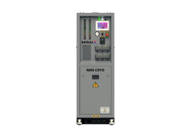
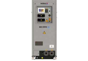
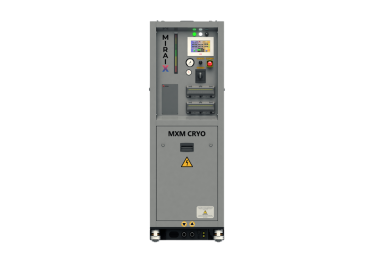
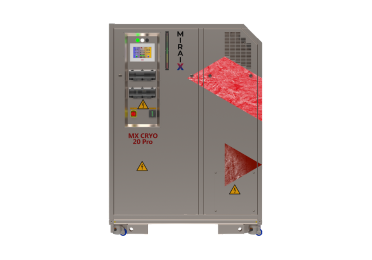
Mirai Intex products and technologies that can be used in production of wafer manufacturing
Mirai Intex, a company renowned for its innovative approach to environmental and industrial technologies, offers a range of products and solutions that can significantly benefit the silicon wafer manufacturing process. Their advanced refrigeration technologies can be seamlessly integrated into various stages of production, from crystal growth to packaging, enhancing efficiency, and sustainability.
In the realm of crystal growth, Mirai Intex's ultra-low temperature refrigeration systems can provide precise temperature control, crucial for the delicate process of growing uniform silicon crystals. This precision ensures the growth of high-quality crystals, fundamental for the semiconductor industry's demand for perfection.
For the doping process, where specific impurities are introduced to alter the electrical properties of silicon, Mirai Intex’s precise cooling solutions can help maintain the exact temperature conditions required for optimal doping outcomes. This precision aids in achieving the desired semiconductor characteristics with higher yield rates.
During the lithography, etching, and deposition stages, where patterns are created and materials are added to the silicon wafer, Mirai Intex’s refrigeration machines can provide clean and controlled environments during its operation, which can minimize contamination risks, ensuring higher quality and reliability of the semiconductor chips. Their technology ensures that the intricate patterns essential for modern chips are flawlessly executed.
Furthermore, in the final stages of metallization and packaging, where connections within the semiconductor are formed and the chip is prepared for integration into electronic devices, Mirai Intex's solutions can enhance the precision and efficiency of these processes. The company’s innovative technologies can help optimize production flow, reduce energy consumption, and lower overall production costs, all while maintaining the high standards of quality required in the semiconductor industry.
By incorporating Mirai Intex products and technologies into the silicon wafer manufacturing process, companies can not only achieve superior quality and efficiency but also embrace greener, more sustainable manufacturing practices. This alignment with environmental sustainability, without compromising on the technological demands of silicon wafer production, positions Mirai Intex as a valuable partner in the advancement of the semiconductor industry.
Frequent questions on the topic
Where are silicon wafers manufactured?
Silicon wafers are manufactured worldwide, with significant production centers in Asia (Taiwan, South Korea, Japan, and China), the United States, and Europe, reflecting the global nature of the semiconductor industry.


