Photolithography in chip making process
What is photolithography and it types
Process of photolithography is a key in semiconductor manufacturing required for etching detailed circuits onto silicon wafers. It is a key tool in microchip (IC) manufacturing, using a sophisticated method of transferring intricate patterns from a photomask to a substrate coated with a light-sensitive chemical photoresist. There are different photolithographically types, depending on the use of ic.
Is there any difference between lithography and photolithography
Very often people can think that lithography is defined as photolithography. Both terms are closely related in printmaking and production, and have distinct differences. Lithography, a traditional printing method, involves creating images on a flat surface, usually stone, using oil-based inks and water. This technique is widely used in fine art and commercial printing. Photolithography, on the other hand, is a more advanced and precise technique used mainly in semiconductor manufacturing. It uses light to transfer a geometric pattern from a photomask to a light-sensitive chemical photoresist on a substrate, usually a silicon wafer.
Where is photolithography used?
Photolithography is mostly used in the semiconductor industry, where it plays a crucial role in the production of microchips and integrated circuits. The process is required to create complex patterns of conductive material on semiconductor wafers, which underpin all electronic devices. In addition to traditional microelectronics, photolithography is also used in the manufacture of microelectromechanical systems (MEMS) including sensors, actuators and microfluidic devices. It is also used in the production of flat panel displays such as those used in smartphones, tablets, and televisions. Also, photolithography finds application in the production of optical devices that manipulate light and are needed in many fields. It has its own sector called optical photolithography.
Why is photolithography important?
It provides high precision and consistency, which is critical for large-scale reproduction of complex patterns in integrated circuits and microchips. Photolithography drives innovation in various sectors including computing, telecommunications and healthcare, contributing significantly to the digital technology industry. Its economic impact is significant, underpinning the multi-billion dollar semiconductor industry and playing a key role in the manufacture of a wide range of electronic devices.
History of development of photolithography
Photolithography machines have played a pivotal role in the technological revolution since their inception in the mid-20th century. Tightly intertwined with the semiconductor industry's emergence, these machines were developed to address the increasing demand for miniaturization and enhanced complexity in electronic circuits.
Introduction of this technology was in the late 1950s, photolithography machines evolved from basic photographic techniques used in printing.
They operated by projecting light through a mask with circuit designs onto a photosensitive semiconductor wafer. This exposure altered the wafer's chemical coating, enabling selective etching to create intricate circuits. Over the decades, advancements in these machines, including improved light sources, photoresists, and alignment processes, have allowed for the creation of chips with ever-smaller features.
This evolution has not only made steps for revolutionizing electronic device manufacturing but also catalyzed rapid technological advancements, leading to the development of increasingly sophisticated and compact electronic devices.
Principles of photolithography
Photolithography is based on several fundamental principles that ensure its critical role in semiconductor fabrication.
- Patterning. Photolithography is based on transferring a specific pattern from a photomask to a substrate, usually a semiconductor wafer. This pattern forms the basis of electronic circuits.
- Application of photoresist. Photoresist, which is a light-sensitive material, is uniformly applied to the substrate. When exposed to light, the photoresist undergoes chemical changes that are necessary to create the pattern on the substrate.
- Exposure and development. A substrate coated with photoresist is exposed to light (e.g., ultraviolet light) through a photomask that bears the desired pattern. The light changes the solubility of the photoresist. The substrate is then developed by washing away either exposed or unexposed areas of photoresist, depending on whether positive or negative photoresist is used.
- Etching. After developing, the exposed areas of the substrate from which the photoresist has been removed are etched away, usually with chemicals or plasma. As a result, the pattern is imprinted into the substrate.
- Removing the remaining photoresist. Finally, the remaining photoresist is removed, leaving the substrate with the pattern ready for further processing.
The principles of photolithography combine chemistry and physics, involving precise control of light, materials and chemicals to create extremely small and complex patterns.
What is a photoresist?
Photoresist is a key light-stable material used in photolithography, a process that is crucial to the creation of microchips and other semiconductor devices. It is a special type of substance that reacts to light and is deposited in a thin layer on a semiconductor wafer. In photolithography, light shines on the photoresist through a patterned mask, changing the photoresist's response to certain chemicals.
Photoresist is very important to photolithography because it allows the creation of very small and precise patterns needed for today's advanced electronic devices.
How does light affect the photoresist?
Which role does light play in this process? During photolithography, when light hits the photoresist, it causes a chemical reaction within the material. This reaction changes the properties of the photoresist in the areas that are exposed to light.
For positive photoresist, exposure to light makes the material more soluble, meaning that exposed areas can be easily washed away with developer solutions.
In negative photoresist, on the other hand, exposure to light makes the material less soluble or harder, so that unexposed areas are washed away during development, leaving the exposed pattern untouched. This selective exposure to light, directed precisely by the pattern of the photomask, is essential. It ensures that only certain areas of the photoresist are changed, enabling the precise patterning required for semiconductor wafers.
The ability of photoresist to respond differently to light is what makes it so valuable in the complex process of microchip fabrication.
How is a pattern formed on a silicon substrate?
The resolution of photolithography is crucial in forming patterns on silicon wafers. Initially, photoresist on the wafer is exposed to light, developing the desired pattern with precise detail enabled by the photolithography's resolution. This pattern is then etched onto the silicon using either wet chemical or dry etching processes, which selectively remove unprotected silicon areas. The final pattern, etched into the silicon, forms the complex circuit networks essential to semiconductor devices. Every step, from light exposure to etching, relies on the fine resolution of photolithography to ensure the accuracy and miniaturization necessary for modern electronic devices.
The basic components of a photolithography system
A photolithography system consists of various fundamental components, each contributing significantly to its operation.
- The first key component is the photomask, which holds the pattern that is transferred to the semiconductor wafer.
- Next is the photoresist, a light-sensitive material applied to the surface of the semiconductor wafer that reacts chemically when exposed to light. An exposure system, including a light source and optical lenses, precisely directs and focuses light through the photomask onto the photoresist.
- The leveling systems are necessary to ensure that the photomask and plate are perfectly positioned relative to each other, which is essential for accurate pattern transfer. In addition, after exposure, a developer solution is used to remove parts of the photoresist that have been altered by light, exposing the pattern.
- Finally, etching equipment is used to engrave the pattern onto the wafer surface.
These components working in unison allow the photolithography system to quaintly etch patterns onto the semiconductor wafers, a fundamental step in microchip manufacturing.
Types of photolithography
Photolithography has several specialized types, each with different levels of complexity and precision.
-
Near Ultraviolet (NUV) photolithography
This type uses near-ultraviolet light to transfer the pattern. NUV lithography is ideal for applications requiring moderate resolution. It is often used in the production of standard microchips due to the balance between resolution and cost effectiveness.
-
Deep Ultraviolet (DUV) photolithography
Deep ultraviolet photolithography allows the creation of much finer details using deep ultraviolet light. This technique is critical for manufacturing advanced semiconductors where higher resolution is required. The shorter wavelength of DUV light allows for smaller parts, making it a better choice for high-performance chips.
-
Extreme Ultraviolet (EUV) photolithography
At the forefront of photolithography technology, EUV lithography uses even shorter wavelengths than DUV. This approach is essential for manufacturing next-generation chips, where unprecedented levels of miniaturization and detail are achieved. EUV lithography is the key to pushing the limits of microchip miniaturization and efficiency.
-
Photolithography in the X-ray range
X-ray photolithography, although less common, provides ultra-high resolution by using X-rays to transfer the pattern. This type is typically used in specialized applications where very fine detail is required. X-ray photolithography is more complex and expensive, but is unrivaled in its ability to create intricate patterns at the microscale.
Each of these types of photolithography plays a role in semiconductor manufacturing and is chosen depending on the resolution required and the complexity of the microchip design.
Current trends in photolithography
In the dynamic field of photolithography, current trends are not only increasing precision and complexity, but also emphasizing the critical role of temperature control in semiconductor manufacturing. A prime example is the move to extreme ultraviolet (EUV) lithography to enable the creation of thinner chip elements, where precise temperature control is key to ensuring optimal exposure and pattern accuracy.
Multilayer patterning techniques, which enable the creation of higher density circuits, also rely heavily on maintaining specific temperature conditions to ensure accuracy and consistency. Improving overlay accuracy and reducing line edge roughness further emphasizes the importance of stable temperature conditions to achieve high quality microchip fabrication.
In addition, advanced computing techniques such as machine learning are increasingly being used to control and optimize temperature parameters during the photolithography process.
These trends emphasize the critical intersection of temperature control with technological advances, enabling the production of faster, more efficient, and more reliable electronic components in the continuously expanding semiconductor industry.
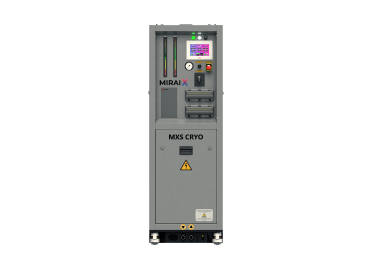
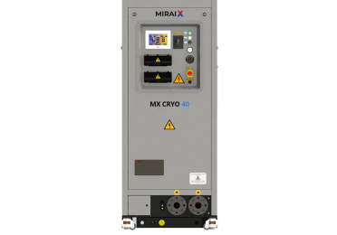
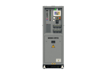
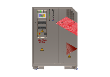
MIRAI Intex products that can be used for microchip production
In microchip manufacturing, accurate temperature control is not just a necessity, it's an art. At MIRAI, we have turned this art into a science with our innovative approach to refrigeration systems.
Our signature equipment offering, MIRAI Cold products, has been a game changer on the world stage. What sets our technology apart is its unique ability to harness the power of air refrigeration in complex procedures such as dry etching in microchip manufacturing. MIRAI helps chip manufacturers with its machines. They have the opportunity to become completely environmentally friendly, reliable and efficient, while saving a good amount of money on machine maintenance. Our MIRAI Cold products don't just improve manufacturing quality, they reinvent the very essence of creating high-tech chips.
We have managed to organically combine these highly desirable attributes, therefore representing what we believe to be the future of chip technology. At MIRAI, we are not just creating products, we are creating a foundation of innovation and environmental awareness for generations to come.
In summary, photolithography is a vital technology in semiconductor manufacturing, playing a crucial role in the miniaturization and efficiency of electronic devices. Its advancement from basic techniques to sophisticated methods like DUV and EUV lithography marks significant progress in electronics. As the backbone of microchip production, photolithography not only drives technological innovation but also significantly impacts the global economy, underscoring its importance in our increasingly digital world.


